Home


Foundries
Improve customer experience and yield, reduce time to volume
![]()
![]()

Chip Designers
Reduce design cycles/iterations for telecommunications, quantum, sensing and other applications
![]()
![]()
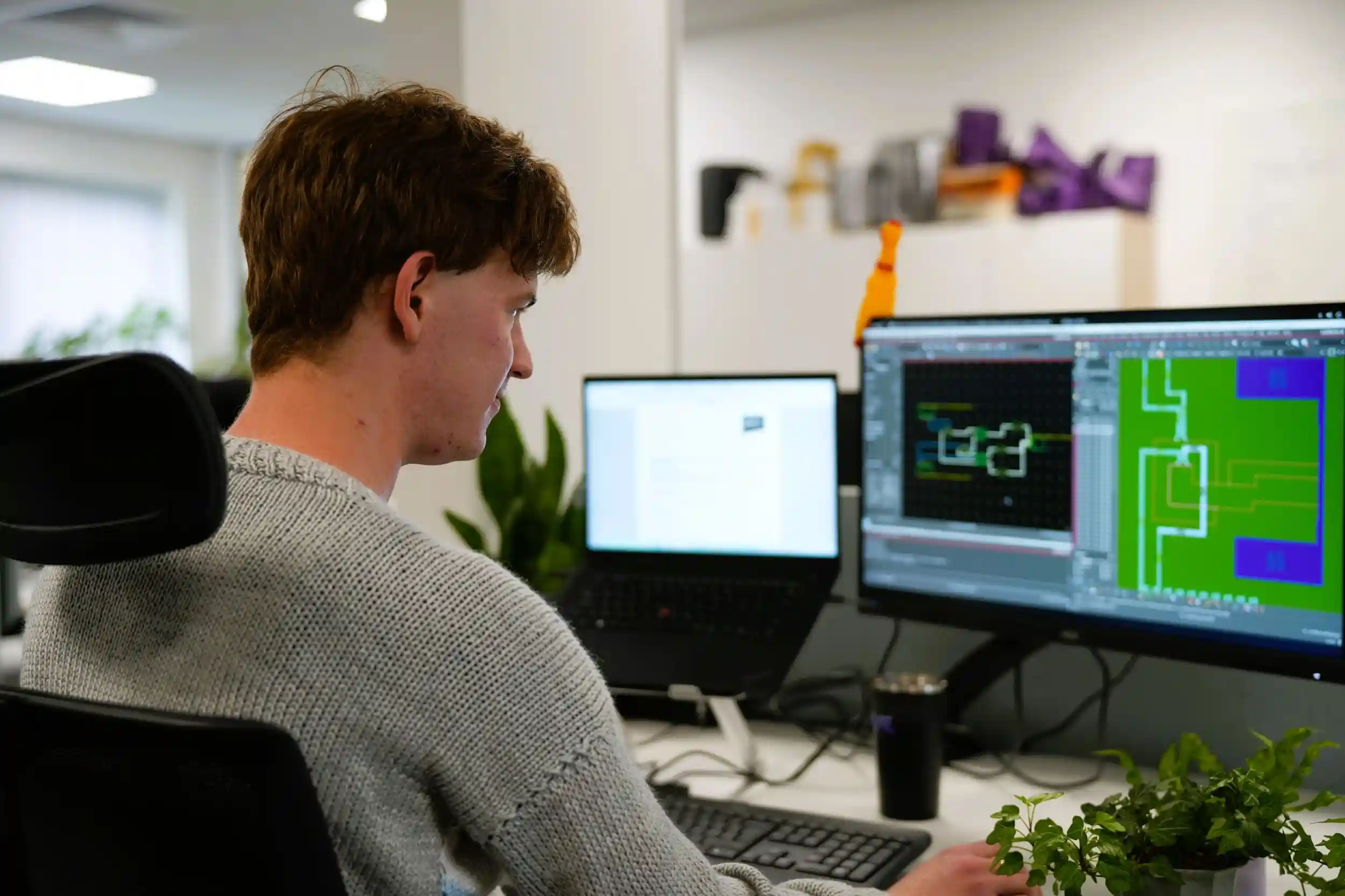
PIC Design Services
Leverage the advantages of PICs in your products with custom PIC architecture development, chip design and more
![]()
![]()

Custom PDK Development
Our proprietary design technology enables us to design a custom or application-specific PDK in weeks. We can create state-of-the-art PDKs for any target material or wavelength to fast-track development for customers working on datacoms, sensing and quantum technologies.
![]()
![]()

PDK Management Platform
Our PDK Management Platform provides a platform to digitally manage PDKs and streamline the designer experience by ensuring PDKs work with leading EDA tools, and provides ready-calculated S-parameters for circuit simulation.
![]()
![]()

PIC Design Services
Our team of photonics and modelling experts offer custom PIC architecture development, chip design, and can manage the fabrication and characterisation process.
![]()
![]()

Packaging & ADKs
We offer easy-to-use reusable packaging templates & Assembly Design Kits (ADKs) which minimise custom development requirements and costs. With our QPICPAC offering, you can have packaged chips in as little as one month.
![]()
![]()
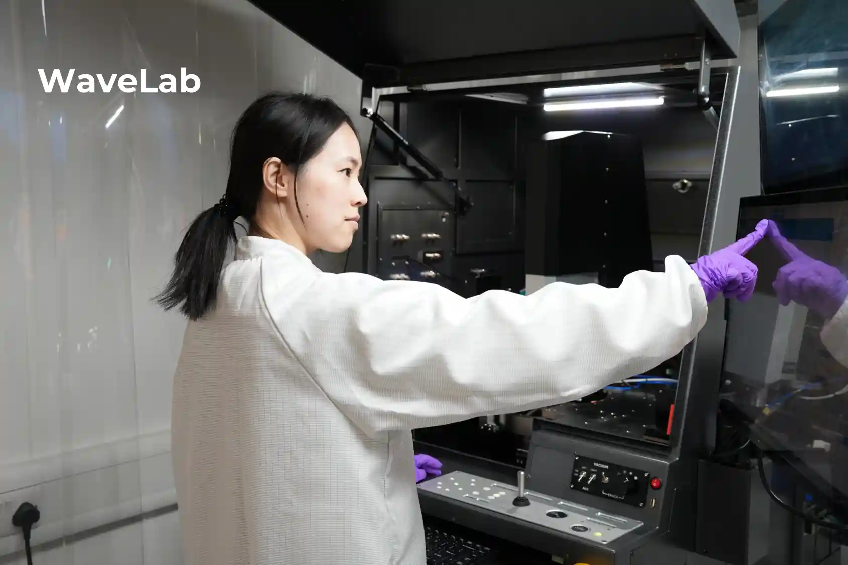
Automated Measurement Service
High-throughput, parallelised measurement capability to test and validate your PIC devices for individual dies or wafers up to 8 inches.
![]()
![]()

Component Libraries and Co-Packaged Optics (CPO) IP
Our IP consists of ready-to-go photonic components, energy-efficient modulator designs, driving and control circuits, and equaliser circuit designs. Our IP is available for licencing and can be accessed through other means.
![]()
![]()